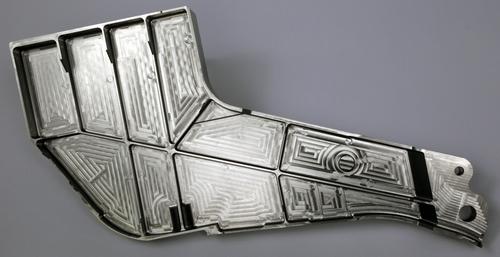

What may be the biggest build volume in additive manufacturing, at least for metal parts, is being done by Sciaky Inc. using a technology that combines an electron beam welding gun with wirefeed additive layering. This direct manufacturing method can make parts as large as 19 ft x 4 ft x 4 ft.
The term “direct manufacturing” is often used to indicate an additive manufacturing process that makes net or near-net production-worthy parts, not prototypes. It’s being used for several aerospace applications, in particular making metal parts for aircraft. For example, we’ve told you about the partnership between Airbus and South African aerostructure manufacturer Aerosud to develop 3D printing methods for large aircraft parts made of titanium. That technology is a form of selective laser sintering (SLS) called laser additive manufacturing (LAM) that forms large, complex structures from titanium powders. The two companies did not disclose the build volume of the machine they are developing.
Sciaky’s direct manufacturing method has a faster deposition rate than the very fine layer deposition of powder metal beds, which are commonly used in SLS. In Sciaky’s process, a fully articulated, movable electron beam wirefeed welding gun deposits metal layers on a substrate plate, Kenn Lachenberg, the company’s applications engineering manager, told us. Metals include titanium, tantalum, inconel, and stainless steel. The machine can deposit anywhere from 7 lb to 20 lb per hour, depending on the object’s shape and material. The process does require a small amount of post-processing finished machining (watch a video of the process below). Lachenberg said:
We’ve incorporated an electron beam, similar to the one we’ve used for conventional electron beam welding, with wire or feedstock placement to add material, a process that’s also available with conventional electron beam welding. In additive manufacturing, since you’re layering metals you have long campaign times and runs, heavy vapor loads, and a higher heat environment. So we rebuilt the electron beam welding machine to handle those issues and give it features that are more feasible for additive manufacturing, such as a closed-loop control system and a faster traveling speed.
We’ve reported on a somewhat similar process that NASA developed for making parts as needed on the International Space Station. Called electron beam freeform fabrication (EBF3), it has a much smaller build volume. The system uses an electron beam gun and a dual-wire feed. On the ground, it’s created parts for the F-35 Joint Strike Fighter’s vertical tails.
The build volumes of SLS and powder metal techniques are limited by the size of the bed to smaller parts. Even laser sintering systems or other electron beam systems may only create a net part of 1 cubic foot, Lachenberg told us. Because Sciaky’s automated gun travels throughout most of the length and width of the chamber, the area where it can deposit material is much less limited.
There’s also no real limit on the size of the machine: the current one is 25 ft x 5 ft x 5 ft, built to fabricate the wing box of an F-14 fighter jet. A typical build rate with titanium is about 15 lb per hour. “We could increase travel speed and wire speed to provide a greater deposition rate, but a lot of work has been qualified at that parameter set,” said Lachenberg. The company is considering increasing both of those speeds, as well as increasing wire diameter, to speed deposition. Sciaky has worked on the development of the process since the late 1990s, when it did feasibility studies with Lockheed Martin. The company is also working on R&D direct manufacturing projects with the US Air Force and the Department of Defense.
Sciaky’s machine and process were displayed recently at the Pennsylvania State University Technology Showcase on Additive Manufacturing. The event was sponsored by the National Additive Manufacturing Innovation Institute (NAMII), launched last August, as well as by DARPA’s Open Manufacturing Program, and the Center for Innovative Materials Processing through Direct Digital Deposition.
Source:
http://www.designnews.com/author.asp?section_id=1392&doc_id=258652&itc=dn_analysis_element&piddl_msgpage=1#msgs


